Nanostructure-based solar cell device concepts
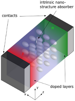 The demand for higher PV energy conversion efficiencies has in the past
decade led to the emergence of a whole new generation of solar cell
concepts, which all aim at exceeding the single junction efficiency
limit through the reduction of fundamental losses. Popular
representatives are the concepts based on enhanced spectrum utilization
and reduced thermalization losses via the use of multiple
junctions,
intermediate bands, multiple exciton generation or hot carrier effects.
While these concepts differ widely in the physical mechanisms
exploited, they have in common that they are largely based on
artificially engineered materials with designed optoelectronic
properties, like semiconductor nano- structures such as quantum wells,
wires and dots, offering size-, geometry- and composition-tunable
characteristics. This deviation from bulk behaviour needs to be taken
into account at the time of describing the device operation mechanisms,
a requirement which may preclude the use of standard macroscopic device
simulation models commonly used in bulk photovoltaics. Similar issues
are encountered in the field of nanostructure based light emitting and
amplifying devices, however, the regime of operation is inverted in
solar cells, since the light needs to be trapped and the charge
carriers are to be extracted. While light-trapping techniques have been
successfully implemented, leading to a substantial
efficiency enhancement, the increase of collection efficiency remains a
critical issue, mainly due to the strong interaction of charge carriers
with their environment and the large number of interfaces associated
with the nanostructures.
The demand for higher PV energy conversion efficiencies has in the past
decade led to the emergence of a whole new generation of solar cell
concepts, which all aim at exceeding the single junction efficiency
limit through the reduction of fundamental losses. Popular
representatives are the concepts based on enhanced spectrum utilization
and reduced thermalization losses via the use of multiple
junctions,
intermediate bands, multiple exciton generation or hot carrier effects.
While these concepts differ widely in the physical mechanisms
exploited, they have in common that they are largely based on
artificially engineered materials with designed optoelectronic
properties, like semiconductor nano- structures such as quantum wells,
wires and dots, offering size-, geometry- and composition-tunable
characteristics. This deviation from bulk behaviour needs to be taken
into account at the time of describing the device operation mechanisms,
a requirement which may preclude the use of standard macroscopic device
simulation models commonly used in bulk photovoltaics. Similar issues
are encountered in the field of nanostructure based light emitting and
amplifying devices, however, the regime of operation is inverted in
solar cells, since the light needs to be trapped and the charge
carriers are to be extracted. While light-trapping techniques have been
successfully implemented, leading to a substantial
efficiency enhancement, the increase of collection efficiency remains a
critical issue, mainly due to the strong interaction of charge carriers
with their environment and the large number of interfaces associated
with the nanostructures.Related group publications:
- Highly transparent front electrodes with metal fingers for p-i-n thin-film silicon solar cells
- Impact of doped microcrystalline silicon oxide layers on crystalline silicon surface passivation
- Optically active defects in SiC, SiOx single layers and SiC/SiOx hetero-superlattices
- Wide gap microcrystalline silicon oxide emitter for a-SiOx:H/c-Si heterojunction solar cells
- Amorphous silicon oxide buffer layers for silicon heterojunction solar cells with microcrystalline silicon oxide contact layers
- Annealing induced defects in SiC, SiOx single layers and SiC/SiOx hetero-superlattices
- Defect passivation by hydrogen reincorporation for silicon quantum dots in SiC/SiOx hetero-superlattice
- Silicon heterojunction solar cell with amorphous silicon oxide buffer and microcrystalline silicon oxide contact layers
- Silicon quantum dot formation in SiC/SiOx hetero-superlattices
- Improvement of hydrogenated microcrystalline (μc−Si:H) single junction solar cells with upconverter at rear side
Quantum-kinetic theory of photovoltaics at the nanoscale
The
conventional approach to the
theoretical description of nanostructure based solar cell devices
consists of a combination of microscopic models for the electronic
structure and optical transitions in the nanostructure with a
macroscopic framework for charge transport. This kind of hybrid
approach can be used to reproduce experimental device characteristics
with remarkable accuracy. However, any situation requiring energy
resolution, non-locality or coherence in the transport process cannot
be described properly, e.g., non-thermalized carrier distributions or
resonant tunneling. To include such processes in a consistent
description, a truly
microscopic picture of carrier transport is to be used.
Hence, for an accurate description of the physics of these novel solar cells based on quantum effects in low dimensional absorbers, the optical transitions and associated carrier generation and recombination processes between the states of the low dimensional absorber are to be treated on equal footing with the processes that provide charge transport in extended states, which amounts to the need for a unified picture of quantum optics and dissipative quantum transport.
The challenge in using a microscopic approach resides in the fact that many modelling requirements that were automatically met by the macroscopic approach, such as, e.g., open boundary conditions, carrier relaxation and non-equilibrium occupation, are very hard to satisfy in a quantum-mechanical picture and have to be addressed explicitly on the basis of scattering states, which results in an adequate description to be found only at the quantum-kinetic level. There, the non-equilibrium Green's function formalism (NEGF), popular in nano- electronics and quantum optics, provides an ideal framework for the formulation of a comprehensive quantum theory of nanostructure based photovoltaic devices.
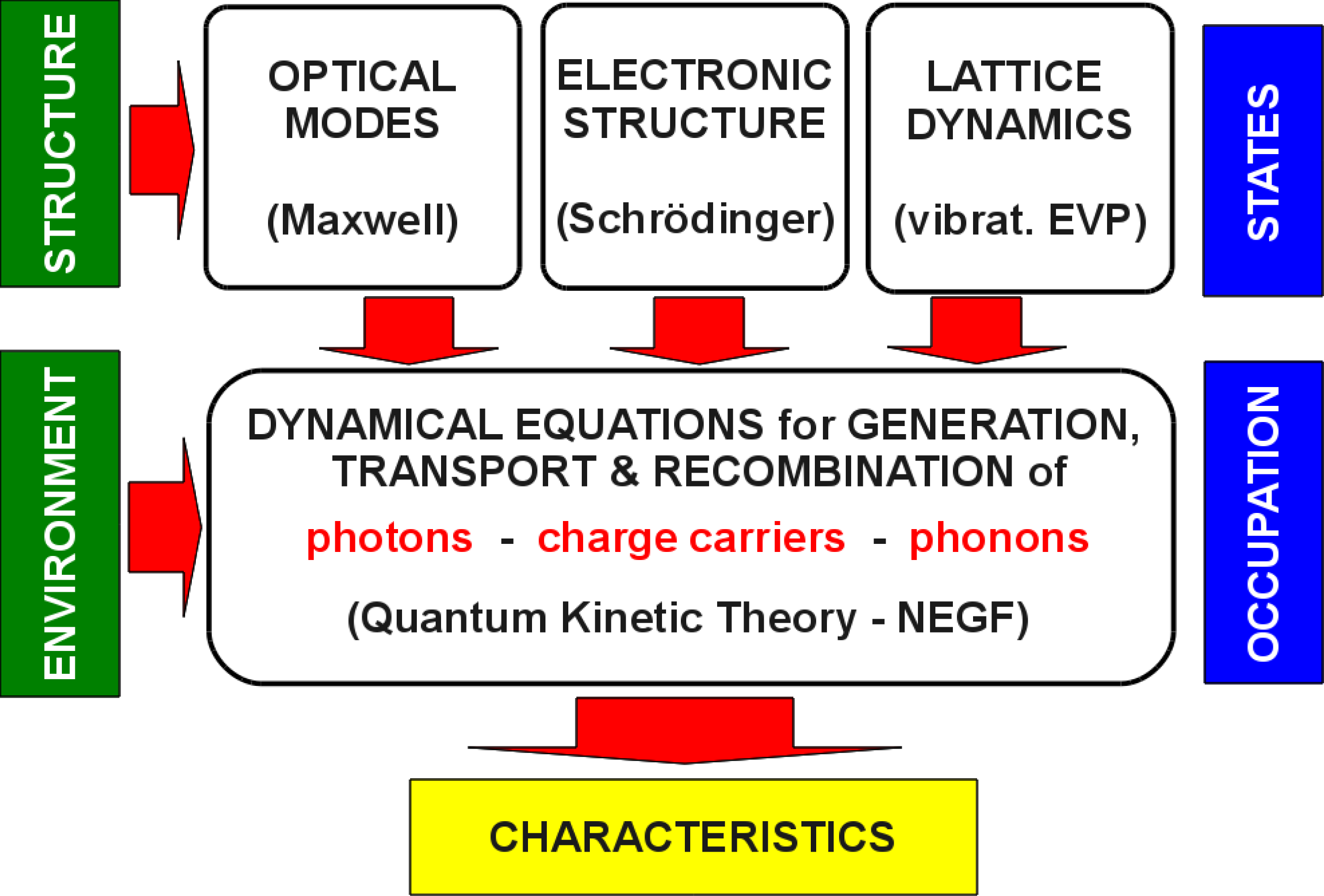
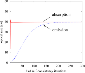
Essentially, the macroscopic steady-state
photovoltaic balance equations are replaced by their microscopic
quantum-kinetic counterparts in terms of Green's functions and
self-energies for charge carriers, based on a general expression of the
total scattering rate (intra- and interband). The Green's functions as
the basic quantities are determined by the steady-state Dyson and
Keldysh equations. While the retarded and advanced Green's functions
are related to the density of states, the correlation functions
additionally contain information on the
(non-equilibrium) occupation of these states. The self-energies on the other hand are scattering functions describing the renormalization of the Green's functions due to coupling to the the environment, in the form of interactions with photons (→ photogeneration, radiative recombination), phonons (→ relaxation,indirect transitions) and other carriers (→ excitons, Auger processes). An additional self-energy term describes injection and extraction of carriers at contacts with arbitrary chemical potential, enabling the treatment of an open non-equilibrium system. The macroscopic photovoltaic device characteristics are obtained from the Green's functions via the respective expressions for steady-state carrier and current densities.
As for the models based on the macroscopic transport equations, the computation of the Green's functions needs to be coupled self-consistently to the determination of the electrostatic potential from Poisson's equation, using the expressions for the carrier densities. Similar sets of equations can also be formulated for the optical and vibrational degrees of freedom (i.e., for photons and phonons), which then provides the desired comprehensive microscopic theory of nanostructure based optoelectronic devices.
Related publications:
- Non-equilibrium Green's function picture of non-radiative recombination of the Shockley-read-Hall type
- Challenges in the NEGF simulation of quantum-well photovoltaics posed by non-locality and localization
- Photovoltaics at the mesoscale: insights from quantum-kinetic simulation
- Quantum-kinetic perspective on photovoltaic device operation in nanostructure-based solar cells
- The non-equilibrium Green's function picture of inelastic processes in nanostructure photovoltaics
- Quantum-kinetic theory of steady-state photocurrent generation in thin films: Coherent versus incoherent coupling
- Non-equilibrium Green's function theory of excitonic effects in the photocurrent response of semiconductor nanostructures
- Quantum-kinetic theory of photocurrent generation via direct and phonon-mediated optical transitions
- Theory and simulation of quantum photovoltaic devices based on the non-equilibrium Green's function formalism
Ultra-thin absorber solar cells
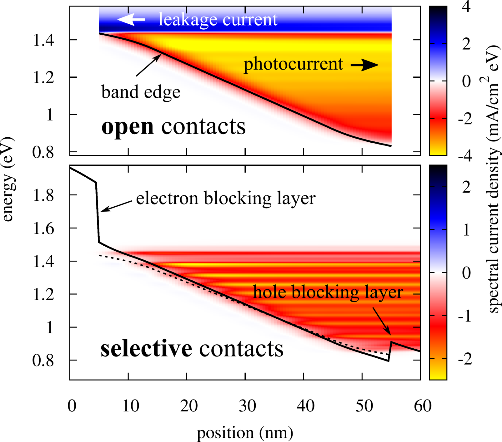
Many high-quality absorber materials such as the direct-gap III-V semiconductors provide the high
energy conversion efficiencies at considerable cost only. One approach to mitigate such expense are the increasingly popular ultrathin-film architectures,
where almost complete absorption of the incident light is achieved in <100 nm via the use of nanophotonic light-trapping. While rigorous optical simulation
has been instrumental for the
development of such devices, no attention was paid to the fact that at such reduced spatial extension, the consideration of the solar cell as electronically
bulk-like object becomes increasingly questionable. Indeed, comparison of the semiclassical device characteristics based on bulk physics with rigorous quantum-kinetic
simulations reveals significant discrepancies in both dark current and photocurrent. There are two deviations from the bulk situation that together explain the observed
discrepancies. On the one hand, the strongly reduced thickness of the space charge region leads to a strong enhancement of the built-in field, which induces electroabsorption
effects and the associated redshift and broadening of the emission spectra. On the other hand, the contact regions span a significant fraction of the entire device and have a
sizable impact on the physical processes in the absorber. For instance, the carrier blocking layers not only prevent leakage currents, but also suppress absorption in the
vicinity of the electrodes.
Related publications:
- Simulation of photon recycling in ultra-thin solar cells
- Microscopic Perspective on Photovoltaic Reciprocity in Ultrathin Solar Cells
- Impact of built-in fields and contact configuration on the characteristics of ultra-thin GaAs solar cells
- Simulation of Ultra-thin Solar Cells Beyond the Limits of the Semi-classical Bulk Picture
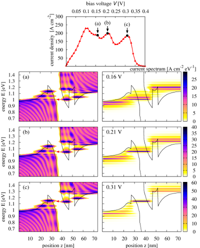
Multi-quantum-well solar cells
The most widely developed and commercially
sucessful photovoltaic
device relying on quantum effects in semiconductor nanostructures is
the quantum well solar cell. In this device, the absorption edge is
red-shifted via the insertion of thin layers of low-band gap material.
The additional photocurrent comes at the cost of increased
recombination in the device regions of reduced band gap. However, the
tunability of the absorption edge allows for a optimized matching to
the solar spectrum in both single and multijunction configurations.
One of the main challenges of the concept is the extraction of carriers at large bias voltage and corresponding low field condition, where carrier escape from deep QW becomes critical. Numerical simulation based on the NEGF formalism provide insight into the role of inelastic scattering and tunneling in the escape process at arbitrary illumination and bias conditions.
One of the main challenges of the concept is the extraction of carriers at large bias voltage and corresponding low field condition, where carrier escape from deep QW becomes critical. Numerical simulation based on the NEGF formalism provide insight into the role of inelastic scattering and tunneling in the escape process at arbitrary illumination and bias conditions.
Related publications:
- Microscopic non-equilibrium theory of quantum well solar cells
- Microscopic theory of coupled quantum well structures in photovoltaics
- Spectral properties of photogenerated carriers in quantum well solar cells
- Microscopic theory and numerical simulation of quantum well solar cells
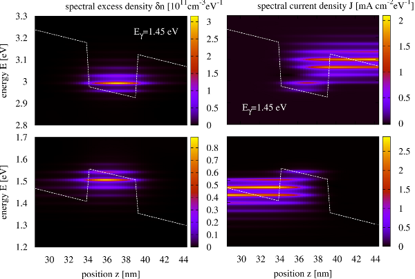
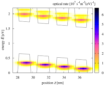
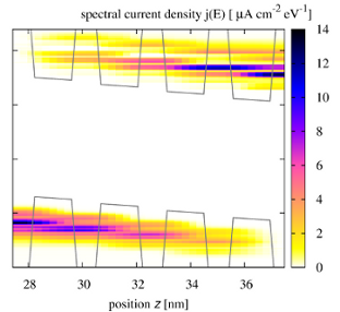
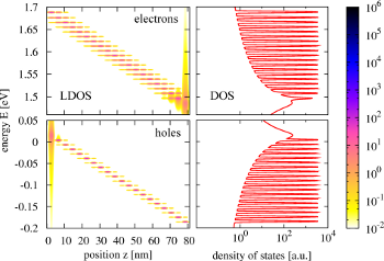
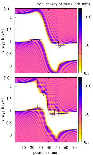
Quantum-well superlattice solar cells
In the absorber designs based on quantum well
superlattices, the latter
do not only provide tunable absorption for charge carrier generation,
but also extended states for charge carrier extraction. However,
internal fields and any kind of disorder result in the breaking of the
miniband structure and corresponding localization of the carrier
wavefunctions, with severe consequences for the transport properties.
The presence of inelastic interactions mitigates some of the
detrimental effects by enabling relaxation between misaligned energy
levels in adjacent wells. The NEGF formalism provides a realistic
picture of current flow from the ballistic regime in extended
superlattice states to sequential tunneling and Wannier-Stark hopping.
Related group publications:
- Photocarrier extraction in GaAsSb/GaAsN type-II QW superlattice solar cells
- Type-II GaAsSb/GaAsN superlattice solar cells
- Theory and simulation of photogeneration and transport in Si-SiOx superlattice absorbers
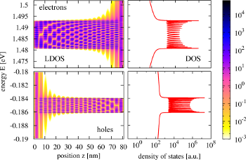
Quantum-dot superlattice solar cells
For certain absorber materials, such as silicon,
one-dimensional
confinement does not provide the required design degree of freedom for
proper tunability of the optical properties, not least due to the fact
that carrier extraction demands the relaxation of carrier confinement
in transport direction. In this situation, nanocrystals absorber
designs are a suitable alternative to the layer systems, as they
possess confinement in three dimensions. However, as in the QWSL case,
carrier localization in the presence of finite fields, i.e. away from
the flat band situation, represents a severe problem, which can only
be partially mitigated by inelastic scattering, as the electron-phonon
interaction is much weaker due to the sparse density of QD states.
Simulation of extended systems with 3D confinement is demanding, wherefore novel multi-scale approaches need to be developed.
Simulation of extended systems with 3D confinement is demanding, wherefore novel multi-scale approaches need to be developed.
Related group publications:
- Effective microscopic theory of quantum dot superlattice solar cells
- Impact of nanostructure configuration on the photovoltaic performance of quantum dot arrays
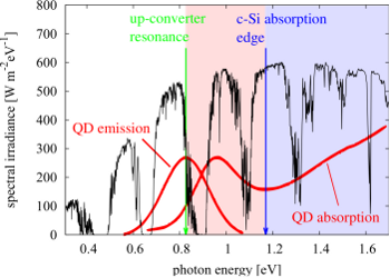
Fluorescent emission of QD
A special type of novel solar cell concepts is
based on spectral tuning
of light to a certain absorber frequency, e.g., for up-conversion
devices. For that purpose, luminescent dyes or nanocrystal QDs are
used.
Due to the importance of the spectral shape of emission, adequate
theories for QD fluorescence should provide physical lineshape. The
line shape is
naturally obtained by using the NEGF formalism to compute the
luminescent response of an electronically closed nanosystem.
Related publications:
Novel tunnel
junction architectures
Most multijunction devices are operated under
massive optical
concentration, resulting in high currents. In this regime, losses at
tunnel junctions between single component cells can become significant.
Novel concepts for the optimization of the tunnel junction
characteristics include architectures based on quantum wells. In these
devices, current flow is strongly affected by the energetic alignement
of bound and quasibound states in the junction region. Again, the NEGF
formalism provides an ideal framework for the investigation of these
nanostructure induced effects.
Related group publications:
- Theoretical investigation of direct and phonon-assisted tunneling currents in InAlGaAs-InGaAs bulk and quantum well interband tunnel junctions for multijunction solar cells
- Rigorous simulation of InAlGaAs-InGaAs bulk and quantum well interband tunnel junctions for multijunction solar cells
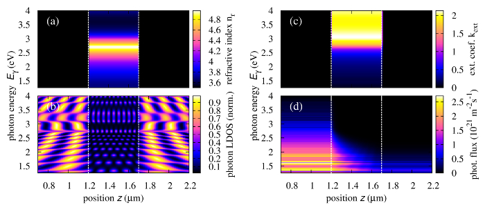
Photonic solar cells
A
wide range of novel solar cell concepts is based on nanophotonic
absorption enhancement, especially in thin film architectures where
insufficient light absorption is a major cause for efficiency
limitation. In the subwavelength regime, the strength of absorption and
emission can be largely tuned via the density and spatial structure of
optical modes. Since solar cell devices are optically open structures,
the relevant resonances are those associated with leaky modes. However,
internal emission couples to all modes available, and consideration of
the full mode structure is essential for a comprehensive assessment of
photon recycling effects.
Extending the NEGF formalism to photon states, the density and occupation of the electromagnetic modes can be determined for arbitrary dielectric structures on equal footing with the optoelectronic properties.
Extending the NEGF formalism to photon states, the density and occupation of the electromagnetic modes can be determined for arbitrary dielectric structures on equal footing with the optoelectronic properties.
Related publications:
Multi-scale simulation of passivated contacts in high-efficiency solar cells
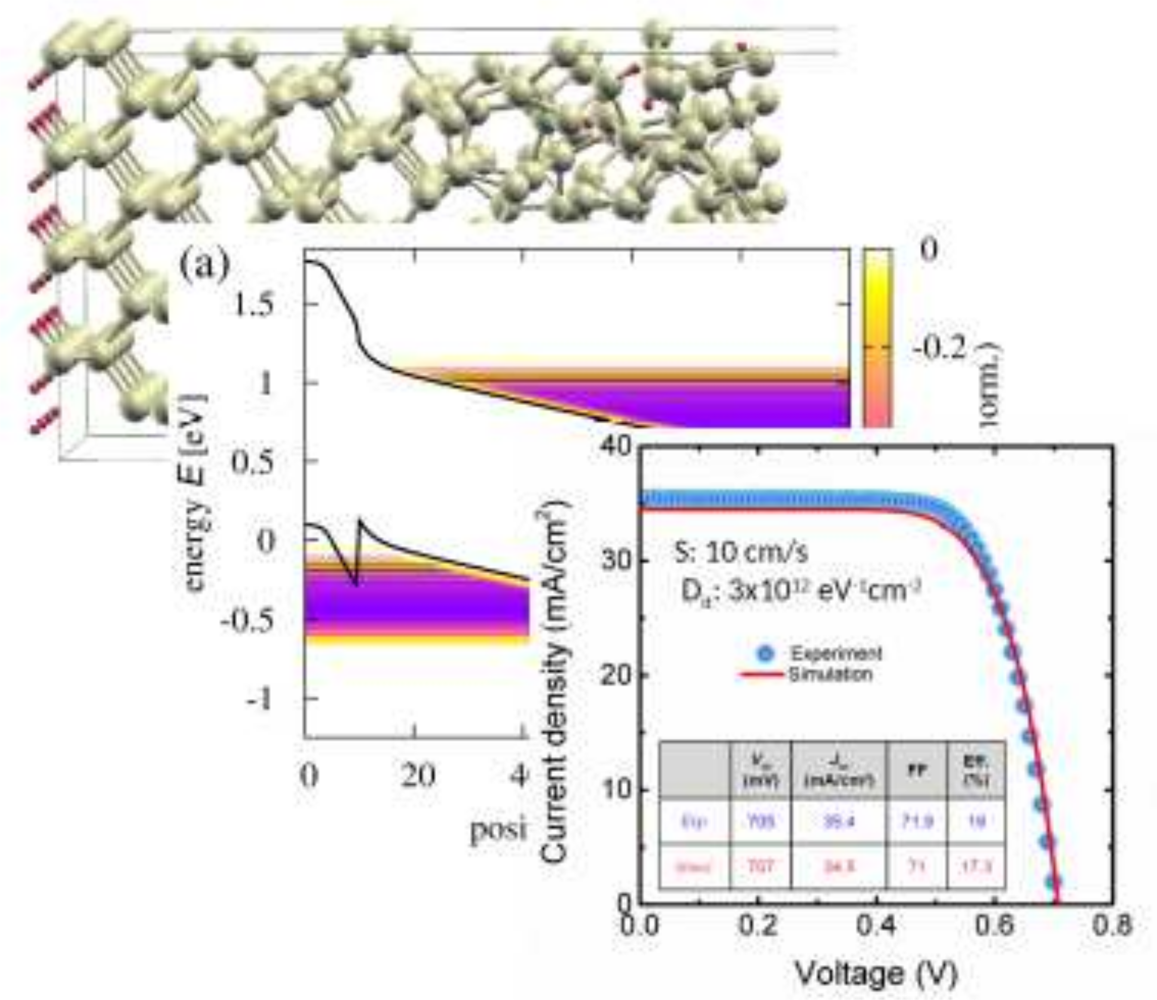 A common aspect of novel silicon solar cell architectures with efficiencies exceeding 25% - such as the silicon heterojunction solar cell (SHJ)
and the tunnel-oxide passivated contact solar cell (TOPCon) - is the central role played by thin-film passivation layers. In the case of the SHJ concept,
the passivation of crystalline silicon wafer surfaces is commonly mediated by a combination of ultra-thin layers of intrinsic hydrogenated amorphous silicon
(a-Si:H →chemical passivation) with highly doped contact layers of hydrogenated microcrystalline silicon(-carbide/oxide) (muc-Si:H, muc-SiC:H or muc-SiOx:H
→field effect passivation).
In the TOPCon concept, a-SiOx:H tunnel oxides provide the desired carrier selectivity at high optical transparency for solar irradiation.
In order to reach efficiencies eta>25%, the physical mechanisms that can potentially limit the photovoltaic performance need to
be understood in detail. Hence, device simulation is required to
resolve the multilayered solar cell architecture in all its complexity, including intricated textures for light trapping and three-dimensional
patterns for interdigitated contacts. Most importantly,
however, an accurate picture of the amorphous-crystalline interface is required regarding transport and recombination of photogenerated charge
carriers in dependence on configurational parameters
such as energies and density of defects, band offsets or doping-induced band bending. Such parameters, on the other hand, should be obtained
from a microscopic resolution of the material at the interface, as
provided by first-principle calculations.
Our multi-scale simulation of passivated contacts in high-efficiency solar cells reflects the above requirements. It starts with the determination
of the atomic and electronic structure from first principles,
based on input from structure and composition and the use of tools such as molecular dynamics and density functional theory. Conventionally,
the microscopic information on the device states is then processed into rates
for generation and recombination as well as mobilities using something like Fermi's Golden Rule, which are then used for macroscopic device
simulation on drift diffusion level. In our case, we insert an additional level
of description at the mesoscale, where the microscopic information provides a parametrization of an effective model for the carrier dynamics
based on quantum-kinetic theory (NEGF formalism).
A common aspect of novel silicon solar cell architectures with efficiencies exceeding 25% - such as the silicon heterojunction solar cell (SHJ)
and the tunnel-oxide passivated contact solar cell (TOPCon) - is the central role played by thin-film passivation layers. In the case of the SHJ concept,
the passivation of crystalline silicon wafer surfaces is commonly mediated by a combination of ultra-thin layers of intrinsic hydrogenated amorphous silicon
(a-Si:H →chemical passivation) with highly doped contact layers of hydrogenated microcrystalline silicon(-carbide/oxide) (muc-Si:H, muc-SiC:H or muc-SiOx:H
→field effect passivation).
In the TOPCon concept, a-SiOx:H tunnel oxides provide the desired carrier selectivity at high optical transparency for solar irradiation.
In order to reach efficiencies eta>25%, the physical mechanisms that can potentially limit the photovoltaic performance need to
be understood in detail. Hence, device simulation is required to
resolve the multilayered solar cell architecture in all its complexity, including intricated textures for light trapping and three-dimensional
patterns for interdigitated contacts. Most importantly,
however, an accurate picture of the amorphous-crystalline interface is required regarding transport and recombination of photogenerated charge
carriers in dependence on configurational parameters
such as energies and density of defects, band offsets or doping-induced band bending. Such parameters, on the other hand, should be obtained
from a microscopic resolution of the material at the interface, as
provided by first-principle calculations.
Our multi-scale simulation of passivated contacts in high-efficiency solar cells reflects the above requirements. It starts with the determination
of the atomic and electronic structure from first principles,
based on input from structure and composition and the use of tools such as molecular dynamics and density functional theory. Conventionally,
the microscopic information on the device states is then processed into rates
for generation and recombination as well as mobilities using something like Fermi's Golden Rule, which are then used for macroscopic device
simulation on drift diffusion level. In our case, we insert an additional level
of description at the mesoscale, where the microscopic information provides a parametrization of an effective model for the carrier dynamics
based on quantum-kinetic theory (NEGF formalism).
Related publications:
- Computational characterization of a-Si:H/c-Si interfaces
- Ab initio study on localization and finite size effects in the structural, electronic, and optical properties of hydrogenated amorphous silicon
- Ab initio description of optoelectronic properties at defective interfaces in solar cells
- Towards a multi-scale approach to the simulation of silicon hetero-junction solar cells